Nanolithographic Methods
Nanosphere Lithography
Nanosphere lithography is based on the self-assembly polystyrene beads that can be commercially purchased. When the beads are covered on a substrate via spin-coating, single or multiple monolayers can be produced. Small openings between the beads can be used to deposit various materials with any technique which allows shadowing effects. Using different bead diameters the separation distance between the openings can be tuned. Please note that nanosphere lithography can only yield hexagonal patterns.
Figure 1 shows periodically ordered nanospheres and metal evaporation on top of the monolayer. After removing the nanospheres only metal in gaps between the spheres remains on the sample.
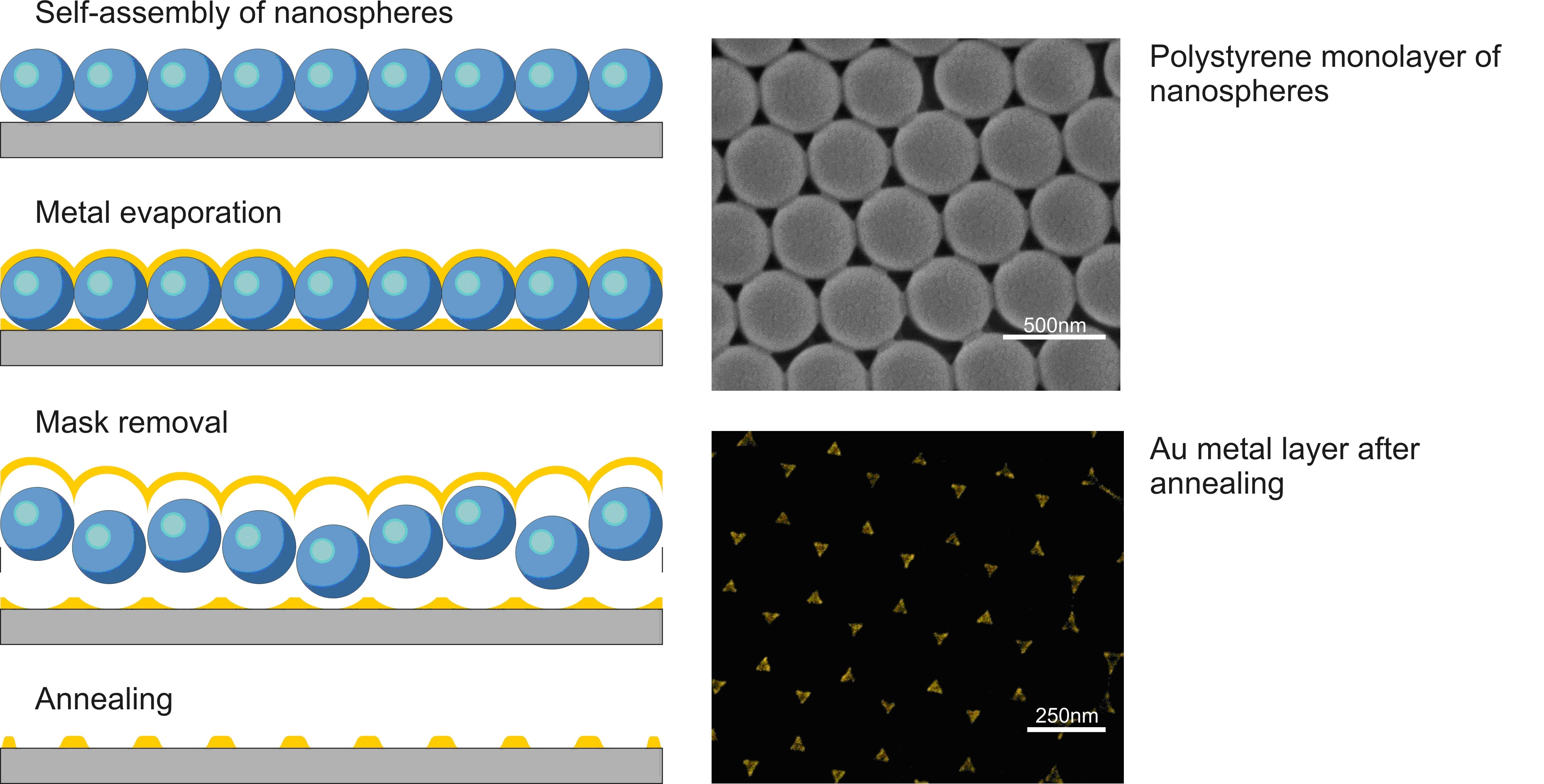 |
| Figure 1: Nano-patterning of metal by nanosphere lithography |
UV Laser Interference Lithography (LIL)
The basic process steps for UV interferences lithography are based on a modified lithographic process using a single mirror. In this process, the incident light and the reflected light from the mirror create a standing wave which can then be used to expose a photosensitive resin. Figure 2 shows the basic setup.
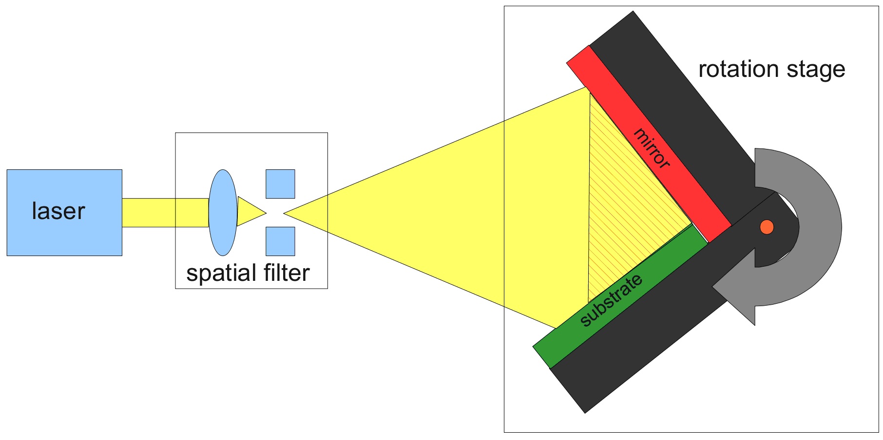 |
| Figure 2: Lloyd’s mirror interferometer – basic setup |
We are able to create hole, trench, line and dot patterns using this patterning technique. In our laboratory, the patterned polymer films are used as a masking layer for the deposition of Au with a standard metal evaporator. The deposited Au dots can be employed as seed layers for ZnO nanowire growth Figure 3 shows the process steps.
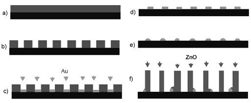 |
| Figure 3: The images show the basic process steps of UV interferences lithography: (a) spinning of resist/anti-reflections coating, (b) exposure or double exposure using UV interference and respective development, (c) deposition of Au by evaporation or sputtering, (d) removal of resist/antireflection layers, (e) pre-annealing of the Au pattern for spherical shape of the dots and (f) growth of the ZnO nanowires. |
Phase Shift Lithography
Near Field Phase Shift Lithography, or NF-PSL for short, is researched and applied intensively for the generation for sub-100 nm patterns in our lab. The method is used for the purposes of nanowire seed structuring and fabrication of nanochannel.
The working principle of NF-PSL is fairly simple. Destructive and constructive interference patterns occurring in sharp edges created on the substrate surface (such as square trenches) create intensity peaks and valleys which are used for exposing positive and negative tone photoresist layers (Figure 4).
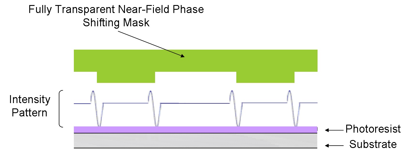 |
| Figure 4. Intensity patterns created by NF-PSL |
Please note that NF-PSL masks are fully transparent and the edges are the only position where the light intensity is modulated.
Instead of the conventional PDMS based NF-PSL photomasks, we produced a novel NF-PSL photomask using borosilicate glass. An SEM view of the produced mask’s surface can be seen below in Figure 5.
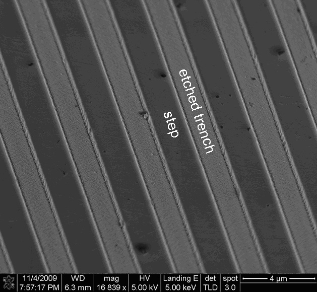 |
| Figure 5: Hard masks have a clear advantage when compared to soft masks. They allow overlay alignment and therefore suitable for multilayer exposure and fabrication. Figure below shows some examples of NF-PSL. |
Using our homemade NS-PSL masks, we can easily generate line and dot patterns as shown in Figure 6.
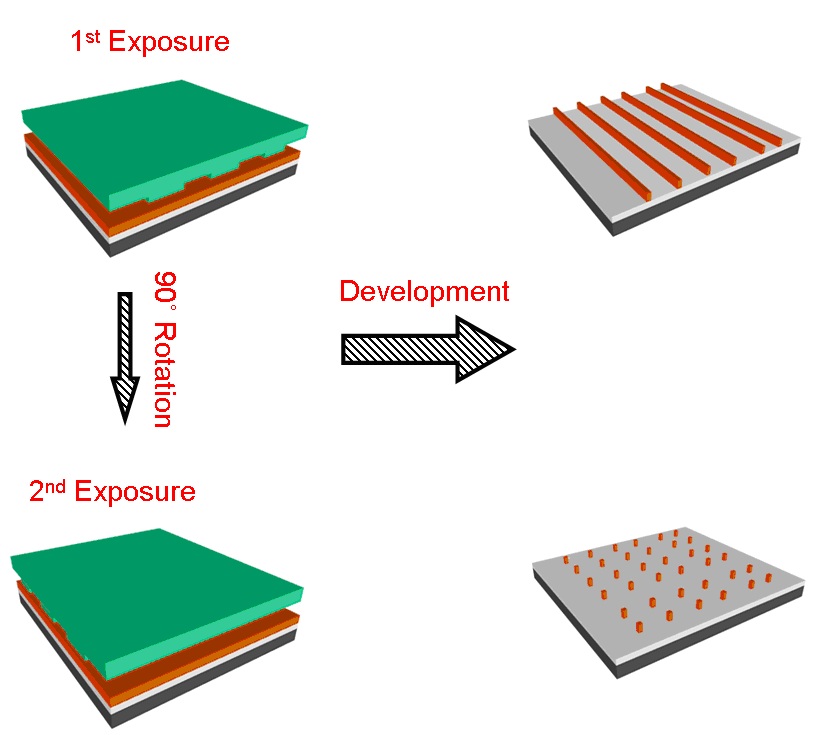 |
| Figure 6. (top) Fabrication of sub-100 nm line patterns with a single NF-PSL exposure, (bottom) 90˚ rotation and second exposure result in dot patterns |
Selection of related publications:
H.J. Fan et al., Superlattices and Microstructures 36, 95 (2004)
D. S. Kim et al., Small 3, 76 (2007)
M. Zacharias et al., Phys. Status Solidi B 247, 2305 (2010)
K. Subannajui et al., Nano Lett 11, 3513 (2011)
F. Güder et al., ACS Applied Materials and Interfaces 12, 3473 (2010)
K. Subannajui et al., Nanotechnolgy 23, 235607 (2012)
Contact
Dr. rer. nat. Firat Güder
Nanotechnologie 01/101
Georges-Köhler-Allee 103
79110 Freiburg i. Br.
Tel.: 0761 / 203 - 7059

