Atomic Layer Deposition
Atomic Layer Deposition (ALD)
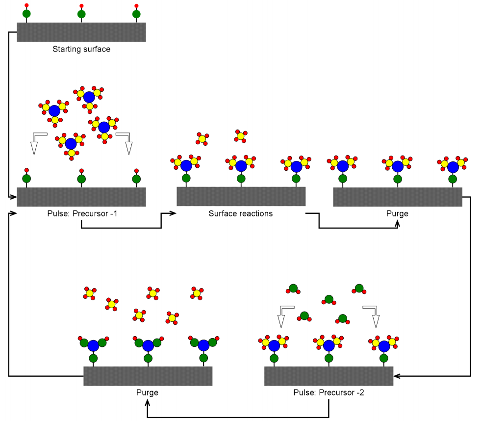
ALD is a sequential chemical vapor deposition technique that is capable of producing high quality, conformal inorganic and hybrid organic-inorganic thin films down to a few angstroms in thickness. In contrast to conventional CVD, in ALD, gas reactions are divided into half-reactions or two separate surface reactions. In other words, in conventional CVD, the reaction gasses are released into the deposition reactor simultaneously in a continuous manner and in ALD, the reaction gasses are pulsed into the reactor separately in a sequential or digital manner to react with the surface species independently. The ALD reaction mechanism is illustrated below.
 |
| A typical ALD process |
Surface modification of nanostructures by ALD
Complex 3D nanostructures can be conformally coated by ALD. An example of a ZnO nanowire coated by Al2O3 can be seen below.
 |
Al2O3 coated ZnO nanowires |
Nano-Kirkendall Effect
Kirkendall effect, a classical metallurgical phenomena, involves formation of voids caused by different diffusivities between a diffusion couple. Diffusion of vacancies compensate the difference in the diffusion rate and the supersaturation of vacancies induce voids on the side of the faster diffusing material.
 |
| VS ZnO nanowire coated with 10 nm ALD Al2O3 and plot of shell thickness vs number of ALD cycles |
ZnO and Al2O3 represent an extreme case of the Kirkendall effect in which only ZnO is the diffusing species. Using this effect, ZnO nanowires can be coated with Al2O3 via atomic layer deposition(ALD) can be annealed and turned into either complete ZnAl2O4 spinel nanotubes or porous ZnAl2O4/ZnO nanostructures. The thickness of the Al2O3 coating can be well tuned using the ALD technique which gives a precise measure of control over porosity of the structure.
 |
| On the left: porous VS ZnO/Al2O3 core-shell nanowire (annealed at 700 C). The shell is converted to ZnAl2O4 spinel - On the right: ZnAl2O4 spinel nanotube (annealed at 800 °C) |
Further related literature: F. Güder, PhD Thesis, 2012, University of Freiburg
ALD based device fabrication methods
Another important aspect of ALD is that it offers the possibility of depositing inorganic thin films at lower temperatures sometimes all the down to room temperature. This is very important for coating of temperature sensitive substrates such as organic structures. Figure below shows 35 nm TiO2 coated photoresist structures at 115 ˚C.
 |
| TiO2 coated AZ 5214 photoresist patterns at 115 ˚C |
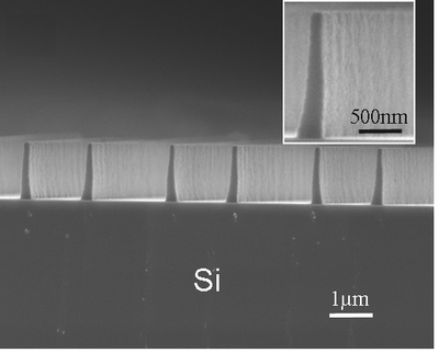
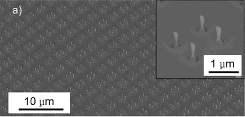
With our novel nanofabrication techniques (like phase shift lithography) we successfully fabricated nanodots homogeneous on wafer scale. Combining anisotropic etching techniques and atomic layer deposition (ALD) we are able to fabricate nanowires of any material in an ordered way. In our laboratory polycrystalline ZnO nanowires can be fabricated on wafer scale suitable for batch fabrication.
 |
| A wafer scale array of ZnO NWs on a (100) Si wafer, and (inset) ALD ZnO NWs with an overetched surface (K. Subannajui et al., Nanotechnolgy 23, 235607 (2012)) |
Selection of related publications:
H. J. Fan et al., Superlattices and Microstructures 36, 95 (2004).
D. S. Kim et al., Small 3, 76 (2007).
M. Zacharias et al., Phys. Status Solidi B 247, 2305 (2010).
K. Subannajui et al., Nano Lett. 11, 3513 (2011).

