
Projects
Phosphorus and boron in nanoscale silicon - investigation of doping and defect mechanism
Project description
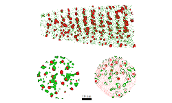
Silicon, whose electronic properties can be controlled via doping with phosphorous and boron, is the basis of manifold technological applications in electronics, optoelectronics, and photovoltaics. Especially the CMOS transistor technology approaches the threshold to dimensions where quantum confinement effects occur. On the nanoscale various problems of semiconductor-physical, thermodynamical, or statistical nature impede the successful and reliable doping of source/drain regions of field effect transistors which appear to prevent further miniaturization. On the other hand, various papers report on successful P- and B-doping of silicon quantum dots (Si QDs) of few nanometers in size. Our recent studies on P-doping of 5 nm Si QDs reproduce the literature reports. However, the combination with detailed structural measurements and statistical analysis (atom probe tomography, synchrotron-based x-way absorption spectroscopy) created doubt, whether the optically and electrically measured changes of the Si QD properties are indeed caused by real P-doping. Our data reveals a rather large number of Patoms per QD, though only a percent fraction seems to be ionised with 2-3 times higher ionisation energies than for bulk-Si. Density functional simulations of P-doped Si approximants reveal no states providing majority carriers for none of the potential configurations. Various states in the vicinity of the band edges occur, however, which represent possible defect- and recombination centers. These states seem to be a feasible explanation for the attenuated photoluminescence and the improved conductance. Based on this preliminary work we want to investigate within this proposal th e Pand B-doping of nanoscale silicon in detail. The major goal is the elucidation of the contradiction between the various literature reports as well as the creation of a comprehensive overview of defect- and doping mechanisms. For this endeavour we possess a sample system which was optimized for several years as well as an extensive tool box of approved structural, optical, and electrical measurement instruments. Considering the importance of future Si-based electronics, the investigation of doping of nanoscale silicon is of utmost priority. The experimental and personnel configuration of this project proposal offers the ideal chance to achieve crucial research results that reveal to which extent classical doping can be employed in future field effect transistor generations and what kind of defect mechanisms have to be expected.
Start/End of project
20.10.2014 until 30.06.2018
Project manager
Hiller D
Contact person
Hiller D
Phone:203-7405
Email:daniel.hiller@imtek.uni-freiburg.de
Partners
Institut für Oberflächen- und Schichtanalytik (IFOS, Kaiserslautern)
Keywords
Nano, Nanotechnology, Materials, Nanomaterials, Nanostructures, Nanocrystals, Phosphorous, Boron, Quantum Confinement, Doping