Current Research
1. Si Nanocrystals
Si Nanocrystals (Si-NC) in oxide and nitride matrix are prepared by plasma enhanced chemical vapour deposition (PECVD) or reactive evaporation. The size of the silicon quantum dots is precisely controlled between 2 and 5 nm via the superlattice approach. Due to quantum confinement effects the bandgap of nanocrystalline silicon is increased from 1.1 eV (bulk-Si) up to 1.7 eV. In addition, Heisenbergs uncertainty principle allows for highly efficient radiative exciton recombination (luminescence) in the Si-NCs despite the still indirect bandgap nature. We investigate fundamental physical properties on the nanoscale as well as applications in photovoltaics and optoelectronics. more |
2. ZnO Nanowires
We are evaluating different methods of nanolithography for the deposition of well ordered Au dot arrays which are then used for nanowire growth by either vapor-liquid-solid growth or vapor-solid growth. The growth conditions are studied which allow the growth of well separated periodically arranged ZnO nanowires for different applications. Our laboratory is equipped with state of the art measuring devices for electrical and optical examinations. We are able to do electrical measurements on single nanowires by the using nanomanipulators within a SEM. In addition, we work on methods for nanowire doping during growth. more |
3. ALD and Surface Modification of Nanostructures and Interfaces
ALD is a sequential chemical vapor deposition technique that is capable of producing high quality, conformal inorganic and hybrid organic-inorganic thin films down to a few angstroms in thickness. more |
4. Controlled Doping of Nanostructures
The realization of nanoscale devices demands new ways of controlled doping as common doping processes fail to meet the requirements in terms of junction depth and abruptness and 3D doping capability. We develop new methods for doping and related characterization methods. more |
5. Nanolithographic Methods
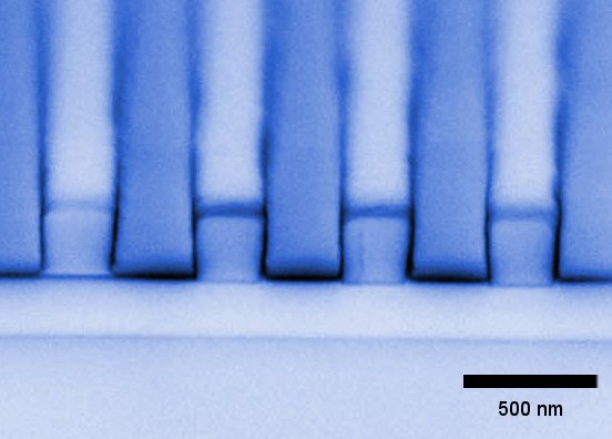
We use comparably cheap patterning methods to obtain nanolines and nanodot arrays on large scale. The following methods are readily applied to various projects: Laser Interference Lithography, Nanosphere Lithography and nanoporous templates |
6. Metal-Assisted Chemical Etching of Silicon
7. Real-Time Nanobiosensors based on Semiconducting Nanostructures


