
ZnO Nanowires
We are evaluating different methods of nanolithography for the deposition of well ordered Au dot arrays which are then used for nanowire growth by either vapor-liquid-solid growth or vapor-solid growth. The growth conditions are studied which allow the growth of well separated periodically arranged ZnO nanowires for different applications. Our laboratory is equipped with state of the art measuring devices for electrical and optical examinations. We are able to do electrical measurements on single nanowires by the using nanomanipulators within a SEM. In addition, we work on methods for nanowire doping during growth.
ZnO Nanowires by vapor deposition technique
We fabricate ZnO nanowires by vapor deposition techniques. The growth of ZnO nanowires can be distinguished between the VS and the VLS growth mode. In our laboratory we use a 1-Zone heating and a 2-Zone heating furnace for the controlled growth of ZnO nanostructures. The 2-Zone heating furnace enables the independent control of substrate and powder source temperature for a homogeneous growth over a range of around 12 cm. We investigate the fundamental properties of ZnO nanowires and their application in electrical, optical and sensor devices.
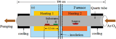 |
| Image of a typical experimental setup (CVD ZnO NW growth) containing a source boat and substrates in a 2-zone growth system. The heating zones can be independently and well controlled enabling a reliable and homogeneous growth over several cm. |
ZnO nanowires are prepared in a chemical vapor deposition approach.
- A source crucible containing a ZnO/C powder mixture is evaporated at high temperatures (e.g. 950 °C). The resulting Zn(g) atoms (the growth species) resulted by a carbothermal reduction mechanism are then transported in the CVD chamber to the substrate for deposition
- Typically there are two growth modes: the vapor-solid (VS) and the vapor-liquid-solid (VLS) growth.
- In the VS case the Zn atoms condensate on a solid catalyst (e.g., Au) at a lower temperature and a preferential deposition happens on energetically favored nucleation sites. The Zn atoms move due to surface diffusion and by self organization the ZnO nanowires grow with a preferential orientation (typically the c-orientation). In case of VS growth the nanowires have a buried Au dot or Au at the root.
- In case of VLS growth the Zn atoms are transported to the metal catalyst and a liquid alloy is formed by adsorption and diffusion mechanisms. After a certain while the solubility is exceeded and the ZnO nanowire precipitates. In case of VLS growth the nanowires typically show an Au dot on the tip. Moreover, the diameter of VLS nanowires can be controlled by the Au dot size.
- We are able to control the growth conditions to switch between VS and VLS growth mechanism. With our systems we can precisely control the carrier gas (Ar) and reaction gas (O2) flows, source and substrate temperatures, and system pressure, to obtain a reliable and reproducible growth.
We investigate: Functional devices based on nanowires like NW based sensors...
|
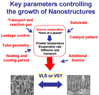
| Schematic of the various parameter influencing the growth |
Selection of related publications:
N. S. Ramgir et al., J. Phys. Chem. C 114, 10323 (2010).
M. Zacharias et al., Phys. Status Solidi B 247, 2305 (2010).
C. Wongchoosuk et al., J. Phys. Chem. C 115, 757 (2011).
A. Menzel et al. J. Phys. Chem. C 116, 5524 (2012).
A. Menzel et al. J. Phys. Chem. Lett. 3, 2815 (2012).
ZnO nanowire growth by solution methods
ALD based ZnO nanowire device fabrication methods
With our novel nanofabrication techniques (like phase shift lithography) we successfully fabricated nanodots homogeneous on wafer scale. Combining anisotropic etching techniques and atomic layer deposition (ALD) we are able to fabricate nanowires of any material in an ordered way. In our laboratory polycrystalline ZnO nanowires can be fabricated on wafer scale suitable for batch fabrication.
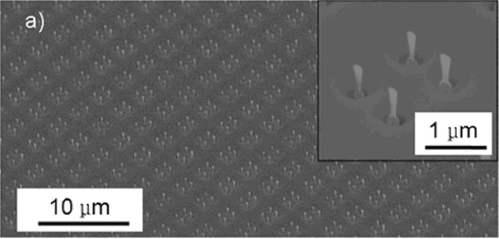 |
| A wafer scale array of ZnO NWs on a (100) Si wafer, and (inset) ALD ZnO NWs with an overetched surface (K. Subannajui et al., Nanotechnolgy 23, 235607 (2012).). |
Selection of related publications:
H. J. Fan et al., Superlattices and Microstructures 36, 95 (2004).
D. S. Kim et al., Small 3, 76 (2007).
M. Zacharias et al., Phys. Status Solidi B 247, 2305 (2010).
K. Subannajui et al., Nano Lett. 11, 3513 (2011).